INFORMATION
Product Features
l BiDi SFF Single Mode
Transceiver
l SC receptacle or with SC/PC or
SC/APC pigtail is optional
l Comply with ITU-T
G.984.2 Class B+
l Compliant
with SFF MSA-2000 And SFF-8472 V10.3
l Single +3.3 Power Supply
l LVPECL Differential Data Inputs
And CML Data Outputs
l LVTTL Signal Detection Output
And LVTTL Burst Control
l Complies with Telcordia
(Bellcore) GR-468-CORE
l 1310 nm Burst Mode Transmitter
and 1490 nm Continuous Mode Receiver
l 1.244 Gbps DFB Laser Diode,
2.488 Gbps APD-TIA Receiver
l Maximal reach 20km
Product Applications
l GPON ONU For P2MP
Application
General
The BD-N12-S20C transceiver with SFF 2*10 package supports typically 1.244 Gbps Tx,2.488 Gbps Rx Asymetric Data Rate for GPON ONU application up to 20km transmission
distance, it’s designed meeting with ITU-T G.984.2 Class B+. SC rececptacle
or SC/PC pigtail is for optical
interface.
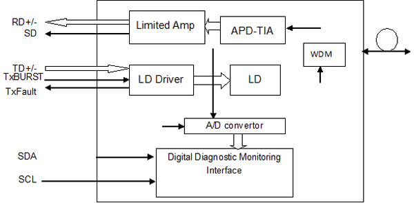
Fig
1 Transceiver Block Diagram
The module provides
digital diagnostic information of its operating conditions and status,
including transmitting power, laser bias, receiver input optical power, module temperature, and supply voltage. Calibration and alarm/warning threshold data
are written and stored in internal memory (EEPROM). The memory map is compatible with SFF-8472,
as shown in Fig. 2. The diagnostic data are raw A/D values and must be
converted to real world units using calibration constants stored in EEPROM
locations 56 – 95 in A2h.
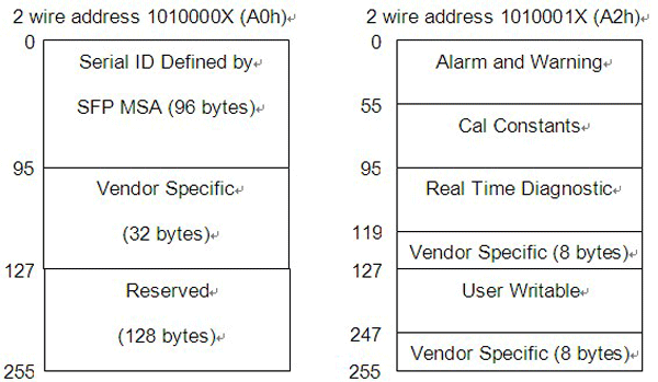
Fig 2 EEPROM Information
Performance Specifications
|
Absolute Maximum Ratings
|
|
Parameter
|
Symbol
|
Min.
|
Max.
|
Unit
|
Note
|
|
Storage Temperature
|
Tst
|
-40
|
+85
|
°C
|
|
|
Operating Case Temperature
|
Tc
|
0
|
70
|
°C
|
V-N1213-S3620C
|
|
-40
|
+85
|
V-N1213-S3620T
|
|
Input Voltage
|
-
|
GND
|
Vcc
|
V
|
|
|
Power Supply Voltage
|
Vcc-Vee
|
-0.5
|
+3.6
|
V
|
|
|
Damage Threshold For
Receiver
|
-
|
-
|
4
|
dBm
|
|
|
Soldering Temperature /
Time
|
-
|
-
|
260/10
|
°C/S
|
|
|
Recommended Operating Conditions
|
|
Parameter
|
Symbol
|
Min.
|
Typical
|
Max.
|
Unit
|
Note
|
|
Power Supply Voltage
|
Vcc
|
3.135
|
3.3
|
3.465
|
V
|
-
|
|
Operating Case Temperature
|
Tc
|
0
|
-
|
70
|
°C
|
V-N1213-S3620C
|
|
-40
|
-
|
85
|
V-N1213-S3620T
|
|
Total Supply Current
|
-
|
-
|
-
|
350
|
mA
|
-
|
|
Optical Specification
|
|
Transmitter
|
|
Parameter
|
Symbol
|
Min.
|
Typ.
|
Max.
|
Unit
|
Note
|
|
Data Rate
|
DR
|
-
|
1.244
|
-
|
Gbps
|
-
|
|
Optical Central Wavelength
|
l
|
1260
|
1310
|
1360
|
nm
|
|
|
Spectral Width (-20dB)
|
Dl
|
-
|
-
|
1
|
nm
|
|
|
Side Mode Suppression
Ratio
|
SMSR
|
30
|
-
|
-
|
dB
|
|
|
Average Optical Output
Power
|
Po
|
0.5
|
-
|
5
|
dBm
|
|
|
Extinction Ratio
|
Er
|
9
|
-
|
-
|
dB
|
-
|
|
Tx Burst ON Time
|
Ton
|
-
|
-
|
12.86
|
ns
|
-
|
|
Tx Burst OFF Time
|
Toff
|
-
|
-
|
12.86
|
ns
|
-
|
|
Rise/Fall Time
|
Tr/Tf
|
-
|
-
|
250
|
ps
|
-
|
|
Average Lauched Power of
Off Transmitter
|
Poff
|
-
|
-
|
-45
|
dBm
|
-
|
|
Output Eye
|
Compliant with ITU-T G.984.2
|
|
Receiver
|
|
Parameter
|
Symbol
|
Min.
|
Typ.
|
Max.
|
Unit
|
Note
|
|
Data Rate
|
DR
|
-
|
2.488
|
-
|
Gbps
|
-
|
|
Operate Wavelength
|
-
|
1480
|
-
|
1500
|
nm
|
-
|
|
Sensitivity
|
Pr
|
-
|
-
|
-28
|
dBm
|
1
|
|
Saturation
|
Ps
|
-8
|
-
|
-
|
dBm
|
1
|
|
SD De-assert Level
|
-
|
-45
|
-
|
-
|
dBm
|
-
|
|
SD Assert Level
|
-
|
-
|
-
|
-28
|
dBm
|
-
|
|
SD Hysteresis
|
-
|
0.5
|
-
|
6
|
dB
|
-
|
|
Optical Return Loss
|
-
|
-
|
-
|
-12
|
dB
|
-
|
|
RSSI Range
|
-
|
-28
|
-
|
-8
|
dBm
|
-
|
|
RSSI Accuracy
|
-
|
-3
|
-
|
+3
|
dB
|
-
|
Note: Minimum Sensitivity and saturation levels
for a 223-1 PRBS. BER≤10-10 , 2.488Gpbs, ER=9dB
|
Electrical Specification
|
|
Transmitter
|
|
Parameter
|
Symbol
|
Min.
|
Typ.
|
Max.
|
Unit
|
Note
|
|
Differential Input Voltage
|
VIN-DIF
|
300
|
-
|
1600
|
mV
|
-
|
|
Tx Burst Input Voltage-Low
|
VIL
|
0
|
-
|
0.8
|
V
|
-
|
|
Tx Burst Input
Voltage-High
|
VIH
|
2.0
|
-
|
Vcc
|
V
|
-
|
|
Receiver
|
|
Parameter
|
Symbol
|
Min.
|
Typ.
|
Max.
|
Unit
|
Note
|
|
Data Output Voltage
Differential
|
VOUT-DIF
|
500
|
-
|
900
|
V
|
-
|
|
Signal Detect Output
Voltage-Low
|
VSD-L
|
0
|
-
|
0.8
|
V
|
-
|
|
Signal Detect Output
Voltage-High
|
VSD-H
|
2.0
|
-
|
Vcc
|
V
|
EEPROM Information
EEPROM Serial ID Memory Contents (A0h)
|
Addr.
(decimal)
|
Field Size
(Bytes)
|
Name of Field
|
Content
(Hex)
|
Content
(Decimal)
|
Description
|
|
0
|
1
|
Identifier
|
02
|
2
|
SFF
|
|
1
|
1
|
Ext. Identifier
|
04
|
4
|
MOD4
|
|
2
|
1
|
Connector
|
0B/01
|
11/01
|
Optical Pigtail /
Receptacle
|
|
3-10
|
8
|
Transceiver
|
00 00 00 00
00 00 00 00
|
00 00 00 00
00 00 00 00
|
Not defined
|
|
11
|
1
|
Encoding
|
03
|
3
|
NRZ
|
|
12
|
1
|
BR, nominal
|
0C
|
12
|
1.25Gbps
|
|
13
|
1
|
Reserved
|
00
|
0
|
-
|
|
14
|
1
|
Length (9um)-km
|
14
|
20
|
20km
|
|
15
|
1
|
Length (9um)
|
C8
|
200
|
20km
|
|
16
|
1
|
Length (50um)
|
00
|
0
|
-
|
|
17
|
1
|
Length (62.5um)
|
00
|
0
|
-
|
|
18
|
1
|
Length (copper)
|
00
|
0
|
-
|
|
19
|
1
|
Reserved
|
00
|
0
|
-
|
|
20-35
|
16
|
Vendor name
|
5A 2D 51 55 49 43
4B 20 20 20 20 20
20 20 20 20
|
90 45 81 85 73
67 75 32 32 32
32 32 32 32 32
32
|
'VCS' (ASCII)
|
|
36
|
1
|
Reserved
|
00
|
0
|
-
|
|
37-39
|
3
|
Vendor OUI
|
00 00 00
|
0 0 0
|
-
|
|
40-55
|
16
|
Vendor PN
|
5A 4E 34 33 34 32 30 39 41
2D 4B xx xx xx 20 20
|
90 78 52 51 52 50 48 57 65
45 75 xx xx xx 32 32
|
V-N1213-S3620C(ASCII)
|
|
56-59
|
4
|
Vendor rev
|
30 30 30 20
|
48 48 48 32
|
“000” (ASCII)
|
|
60-61
|
2
|
Wavelength
|
05 1E
|
05 30
|
1310
|
|
62
|
1
|
Reserved
|
00
|
0
|
-
|
|
63
|
1
|
CC BASE
|
-
|
-
|
Check sum of bytes 0 - 62
|
|
64
|
1
|
Reserved
|
00
|
0
|
|
|
65
|
1
|
Options
|
1A
|
26
|
|
|
66
|
1
|
BR, max
|
00
|
0
|
-
|
|
67
|
1
|
BR, min
|
00
|
0
|
-
|
|
68-83
|
16
|
Vendor SN
|
-
|
-
|
ASCII
|
|
84-91
|
8
|
Vendor date
|
-
|
-
|
Year (2 bytes), Month (2 bytes), Day (2
bytes)
|
|
92
|
1
|
DDM Type
|
58/68
|
88/104
|
External/Internal
Calibrated
|
|
93
|
1
|
Enhanced Option
|
B0
|
176
|
LOS, TX_FAULT and
Alarm/warning flags implemented
|
|
94
|
1
|
SFF-8472 Compliance
|
03
|
3
|
SFF-8472 Rev 10.3
|
|
95
|
1
|
CC EXT
|
-
|
-
|
Check sum of bytes 64 - 94
|
|
96-255
|
160
|
Vendor spec
|
|
|
|
Alarm and Warning Thresholds (Serial ID A2H)
|
Parameter(Unit)
|
C Temp
(℃)
|
I Temp
(℃)
|
Voltage
(V)
|
Bias
(mA)
|
TX Power
(dBm)
|
RX Power
(dBm)
|
|
High Alarm
|
100
|
100
|
3.6
|
90
|
5
|
-8
|
|
Low Alarm
|
-10
|
-40
|
3
|
0
|
0.5
|
-28
|
|
High Warning
|
95
|
95
|
3.5
|
70
|
4
|
-9
|
|
Low Warning
|
0
|
-30
|
3.1
|
0
|
1
|
-27
|
Digital Diagnostic Monitor Accuracy
|
Parameter
|
Unit
|
Accuracy
|
Range
|
Calibration
|
|
Tx Optical Power
|
dB
|
±3
|
Po: -Pomin~Pomax dBm, Recommended operation
conditions
|
External/Internal
|
|
Rx Optical Power
|
dB
|
±3
|
Pi: Ps~Pr dBm, Recommended operation
conditions
|
External/Internal
|
|
Bias Current
|
%
|
±10
|
Id: 1-100mA, Recommended operating
conditions
|
External/Internal
|
|
Power Supply Voltage
|
%
|
±3
|
Recommended operating conditions
|
External/Internal
|
|
Internal Temperature
|
℃
|
±3
|
Recommended operating conditions
|
External/Internal
|
PIN Diagram
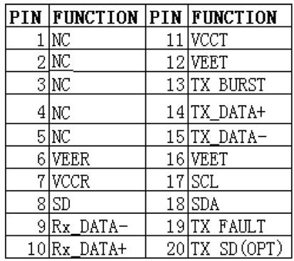
PIN Description
|
Pin No.
|
Name
|
Description
|
|
1
|
NC
|
|
|
2
|
NC
|
|
|
3
|
NC
|
|
|
4
|
NC
|
|
|
5
|
NC
|
|
|
6
|
VEER
|
Receiver Ground
|
|
7
|
VCCR
|
Receiver Power Supply
|
|
8
|
SD
|
Signal Detect Output. H--Normal
Operation; L--Los Of Signal
|
|
9
|
Rx_DATA-
|
Receiver Data Output Negative
|
|
10
|
Rx_DATA+
|
Receiver Data Output Positive
|
|
11
|
VCCT
|
Transmitter Power Supply
|
|
12
|
VEET
|
Transmitter Ground
|
|
13
|
TX_BURST
|
Transmitter Burst Mode Control.
Assert High when Burst on
|
|
14
|
TX_DATA+
|
Transmitter Data Input Positive
|
|
15
|
TX_DATA-
|
Transmitter Data Input Negative
|
|
16
|
VEET
|
Transmitter Ground
|
|
17
|
SCL
|
I2C Serial Clock
|
|
18
|
SDA
|
I2C Serial Data
|
|
19
|
TX FAULT
|
Transmitter Fault
|
|
20
|
TX SD
|
Tx Transmitter State Indication, assert When Tx ON. Optional
|
Recommended Circuit
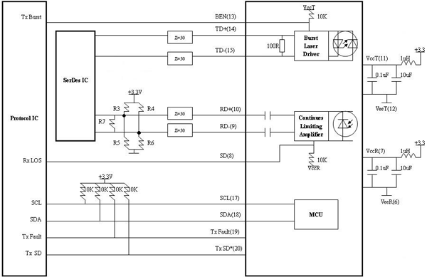
Note:
Tx:DC coupled internally.
Rx:AC coupled internally.
Input stage in SerDes IC
with internal bias to Vcc-1.3V
R3=R4=R5=R6=N.C, R7=100Ω
Input stage in SerDes IC
without internal bias to Vcc-1.3V
R3=R4=82Ω,R5=R6=130Ω,R7=N.C
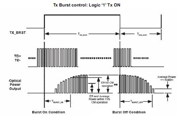
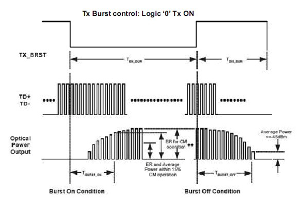
Burst Mode Sequence Definition
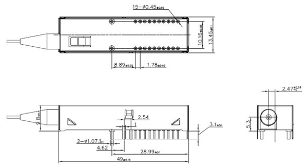
Package Diagram
Change History
|
Version
|
Change
Description
|
Issued
By
|
Checked By
|
Appoved
By
|
Release Date
|
|
A
|
Initial release
|
Licc
|
|
|
2014-02-10
|
|
|
|
|
|
|
|
Ordering information
Related Products
