INFORMATION
BD-QSFP-CD10 is 40Gb/s QSFP+ 10km Optical Transceiver which has Four-Channel, Pluggable, Parallel, Fiber-Optic QSFP+ Transceiver for InfiniBand QDR/DDR/SDR, 10G/8G/4G/2G fiber channel. and SAS Applications. The QSFP full-duplex optical module offers 4 independent transmit and receive channels, each capable of 10.3Gbps operation for an aggregate data rate of 40Gbps 10km using single mode fiber. These modules are designed to operate over single mode fiber systems using 1310nm DFB laser array. An optical fiber ribbon cable with an MPO/MTPTM connector can be plugged into the QSFP module receptacle. QSFP+ PSM LR4 is one kind of parallel transceiver which provides increased port density and total system cost savings.
Product Features
● Four-channel full-duplex transceiver modules
● Transmission data rate up to 11.2Gbit/s per channel
● Up to 10km transmission of single mode fiber
● DFB laser array inside
● Low power consumption <2.5W,
● Operating case temperature:0°C to +70°C
● 3.3V power supply voltage
● RoHS 6 compliant
● Hot Pluggable QSFP form factor
● Single MPO connector receptacle
● Built-in digital diagnostic function
Applications
● InfiniBand QDR, DDR and SDR
● 40G Ethernet
● Proprietary High Speed Interconnections
● Data center
Absolute Maximum Ratings
Parameter
|
Symbol
|
Min.
|
Max.
|
Unit
|
Note
|
Supply Voltage
|
Vcc
|
-0.3
|
3.6
|
V
|
|
Storage Temperature
|
TS
|
-40
|
85
|
°C
|
|
Relative Humidity
|
RH
|
0
|
85
|
%
|
|
Damage Threshold, per Lane
|
DT
|
3.4
|
|
dBm
|
|
Note: Stress in excess of the maximum absolute ratings can cause permanent damage to the transceiver.
General Operating Characteristics
Parameter
|
Symbol
|
Min
|
Typ
|
Max
|
Units
|
Note
|
Bit Rate per Lane
|
BR
|
|
|
10.313
|
Gb/s
|
1
|
Bit Error Ratio
|
BER
|
|
|
10-12
|
|
2
|
Distance on SMF
|
D1
|
|
|
10
|
Km
|
3
|
Notes:
1. Compliant with 40G Ethernet. Compatible with 1/10 Gigabit Ethernet and 1/2/4/8/10G Fibre Channel.
2. Tested with a PRBS 231-1 test pattern.
3. Per 40GBASE-LR4, IEEE 802.3ba.
Optical Characteristics (TOP(C) = 0 to 70 ℃,VCC = 3.13 to 3.47 V)
Parameter
|
Symbol
|
Min.
|
Typ
|
Max.
|
Unit
|
Note
|
Transmitter
|
Operating Wavelength
|
λc
|
1270
|
1310
|
1350
|
nm
|
|
Ave. output power
|
PAVE
|
-5.2
|
|
+1
|
dBm
|
|
Difference in launch power
between any two lanes (OMA)
|
DL
|
|
|
5
|
dB
|
|
Extinction Ratio
|
ER
|
3.5
|
|
|
dB
|
|
Peak power, each lane
|
PP
|
|
|
4
|
dBm
|
|
Dispersion penalty, each lane
|
TDP
|
|
|
3.5
|
dB
|
|
Average launch power of OFF
transmitter, each lane
|
POFF
|
|
|
-30
|
dB
|
|
Eye Mask coordinates:
X1, X2, X3, Y1, Y2, Y3
|
SPECIFICATION VALUES
0.23, 0.34, 0.43, 0.27, 0.35, 0.4
|
Hit Ratio =
5x10⁻⁵
|
Receiver
|
Operating Wavelength
|
λc
|
1270
|
|
1350
|
nm
|
|
Stressed receiver sensitivity in OMA(OLSQ854XM-CDS1)
|
PSEN1
|
|
|
-12.5
|
dBm
|
3
|
Average Receive Power,each lane
|
PAVE
|
-11
|
|
+2.4
|
dBm
|
|
Receiver Reflectance
|
Rrx
|
|
|
-12
|
dB
|
|
LOS Assert
|
Pa
|
-30
|
|
|
dBm
|
|
LOS De-assert
|
Pd
|
|
|
-15
|
dBm
|
|
LOS Hysteresis
|
Pd-Pa
|
0.5
|
|
|
dB
|
|
Notes:
1. Measured with conformance test signal at TP3 for BER = 10-12 Receiver Characteristics
Pin Defintion And Functions
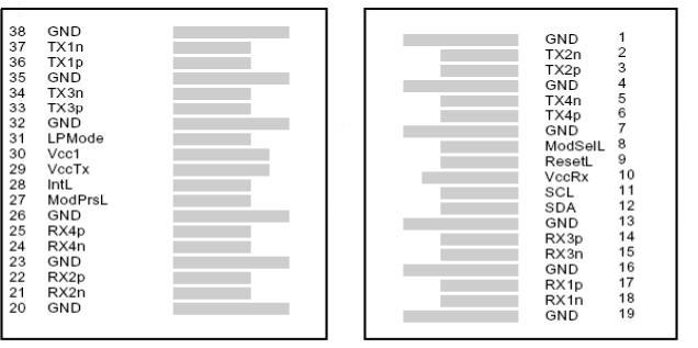
Top side Bottom side
Pin
|
Symbol
|
Name/Description
|
Notes
|
1
|
GND
|
Ground
|
1
|
2
|
Tx2n
|
Transmitter Inverted Data Input
|
|
3
|
Tx2p
|
Transmitter Non-Inverted Data Input
|
|
4
|
GND
|
Ground
|
1
|
5
|
Tx4n
|
Transmitter Inverted Data Input
|
|
6
|
Tx4p
|
Transmitter Non-Inverted Data Input
|
|
7
|
GND
|
Ground
|
1
|
8
|
ModSelL
|
Module Select
|
1
|
9
|
ResetL
|
Module Reset
|
|
10
|
Vcc Rx
|
+3.3 V Power supply receiver
|
|
11
|
SCL
|
2-wire serial interface clock
|
|
12
|
SDA
|
2-wire serial interface data
|
|
13
|
GND
|
Ground
|
1
|
14
|
Rx3p
|
Receiver Non-Inverted Data Output
|
|
15
|
Rx3n
|
Receiver Inverted Data Output
|
|
16
|
GND
|
Ground
|
1
|
17
|
Rx1p
|
Receiver Non-Inverted Data Output
|
|
18
|
Rx1n
|
Receiver Inverted Data Output
|
|
19
|
GND
|
Ground
|
1
|
20
|
GND
|
Ground
|
1
|
21
|
Rx2n
|
Receiver Inverted Data Output
|
|
22
|
Rx2p
|
Receiver
|
Non-Inverted
|
22
|
Rx2p
|
Receiver Non-Inverted Data Output
|
|
23
|
GND
|
Ground
|
1
|
24
|
Rx4n
|
Receiver Inverted Data Output
|
|
25
|
Rx4p
|
Receiver Non-Inverted Data Output
|
|
26
|
GND
|
Ground
|
1
|
27
|
ModPrsL
|
Module Present
|
|
28
|
IntL
|
Interrupt
|
|
29
|
Vcc Tx
|
+3.3 V Power supply transmitter
|
|
30
|
Vcc1
|
+3.3 V Power S
upply
|
|
31
|
LPMode
|
Low Power Mode
|
|
32
|
GND
|
Ground
|
1
|
33
|
Tx3p
|
Transmitter Non-Inverted Data Input
|
|
34
|
Tx3n
|
Transmitter Inverted Data Input
|
|
35
|
GND
|
Ground
|
1
|
36
|
Tx1p
|
Transmitter Non-Inverted Data Input
|
|
37
|
Tx1n
|
Transmitter Inverted Data Input
|
|
38
|
GND
|
Ground
|
1
|
Notes:
1. Circuit ground is internally isolated from chassis ground.
Other Pin Descriptions:
ModSelL Pin
The ModSelL is an input pin. When held low by the host, the module responds to 2-wire serial communication commands. The ModSelL allows the use of multiple QSFP modules on a single 2-wire interface bus. When the ModSelL is “High”, the module will not respond to any 2-wire interface communication from the host. ModSelL has an internal pull-up in the module.
ResetL Pin
Reset. LPMode_Reset has an internal pull-up in the module. A low level on the ResetL pin for longer than the minimum pulse length (t_Reset_init) initiates a complete module reset, returning all user module settings to their default state. Module Reset Assert Time (t_init) starts on the rising edge after the low level on the ResetL pin is released. During the execution of a reset (t_init) the host shall disregard all status bits until the module indicates a completion of the reset interrupt. The module indicates this by posting an IntL signal with the Data_Not_Ready bit negated. Note that on power up (including hot insertion) the module will post this completion of reset interrupt without requiring a reset.
LPMode Pin
Rayoptek PSM IR4operate in the low power mode (less than 1.5 W power consumption) This pin active high will decrease power consumption to less than 1W.
ModPrsL Pin
ModPrsL is pulled up to Vcc on the host board and grounded in the module. The ModPrsL is asserted “Low” when the module is inserted and deasserted “High” when the module is physically absent from the host connector.
IntL Pin
IntL is an output pin. When “Low”, it indicates a possible module operational fault or a status critical to the host system. The host identifies the source of the interrupt by using the 2-wire serial interface. The IntL pin is an open collector output and must be pulled up to Vcc on the host board.
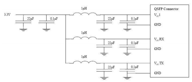
Power Supply Filtering
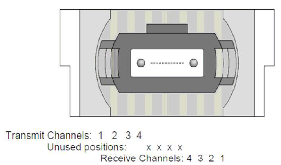
Optical Interface Lanes and Assignmen
The optical interface port is a male MPO connector .The four fiber positions on the left as shown in below, with the key up, are used for the optical transmit signals (Channel1 through4). The fiber positions on the right are used for the optical receive signals(Channel 4 through 1). The central four fibers are physically present.
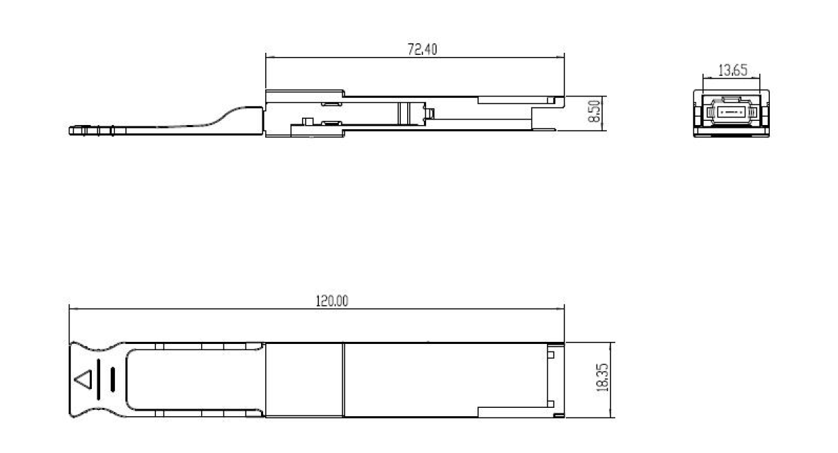
Package Dimensions
Ordering Information
Part Number
|
Description
|
BD-QSFP-CD10
|
QSFP+,40Gb/s, CWDM wavelength 1310nm(4x10G) 10Km, 0~70℃ LC
|
Ordering information
Related Products
